PCB design and selection
تفاصيل العمل

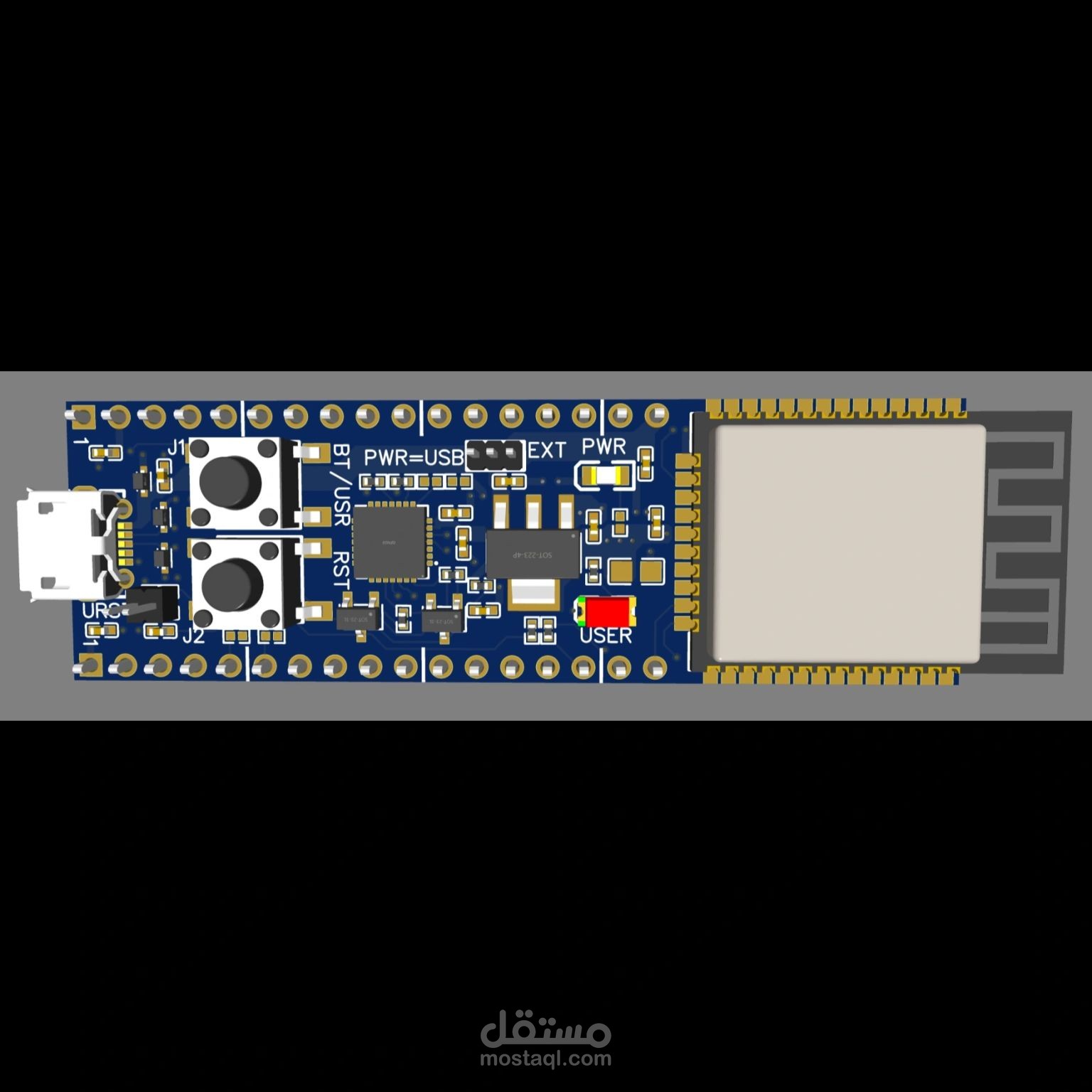
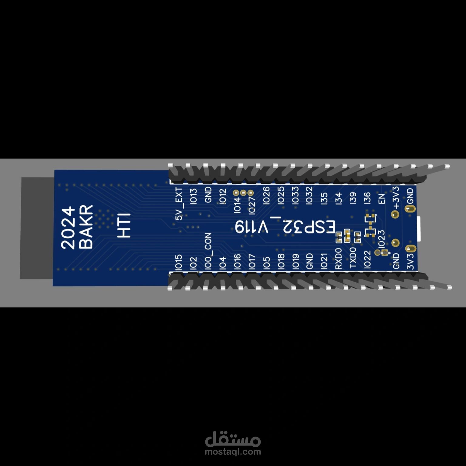
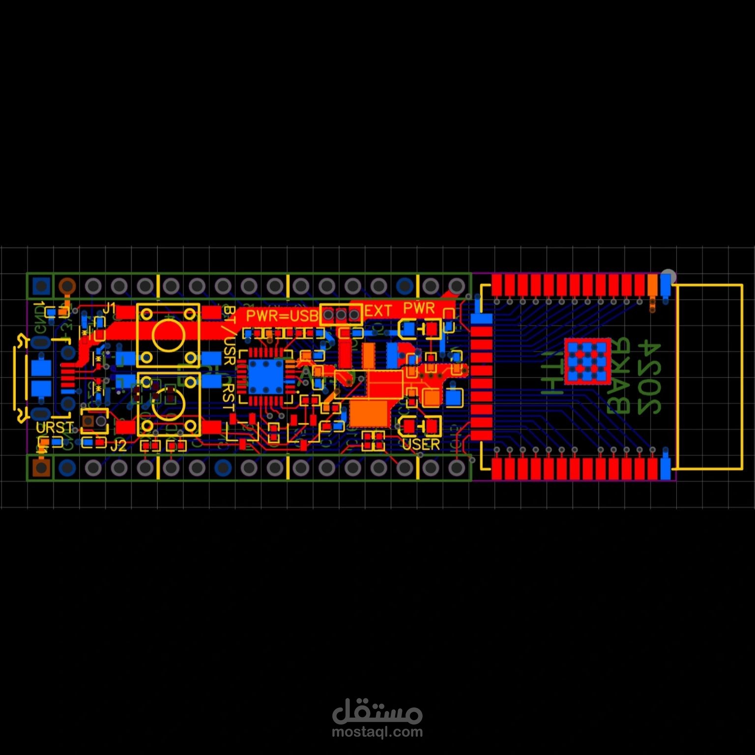
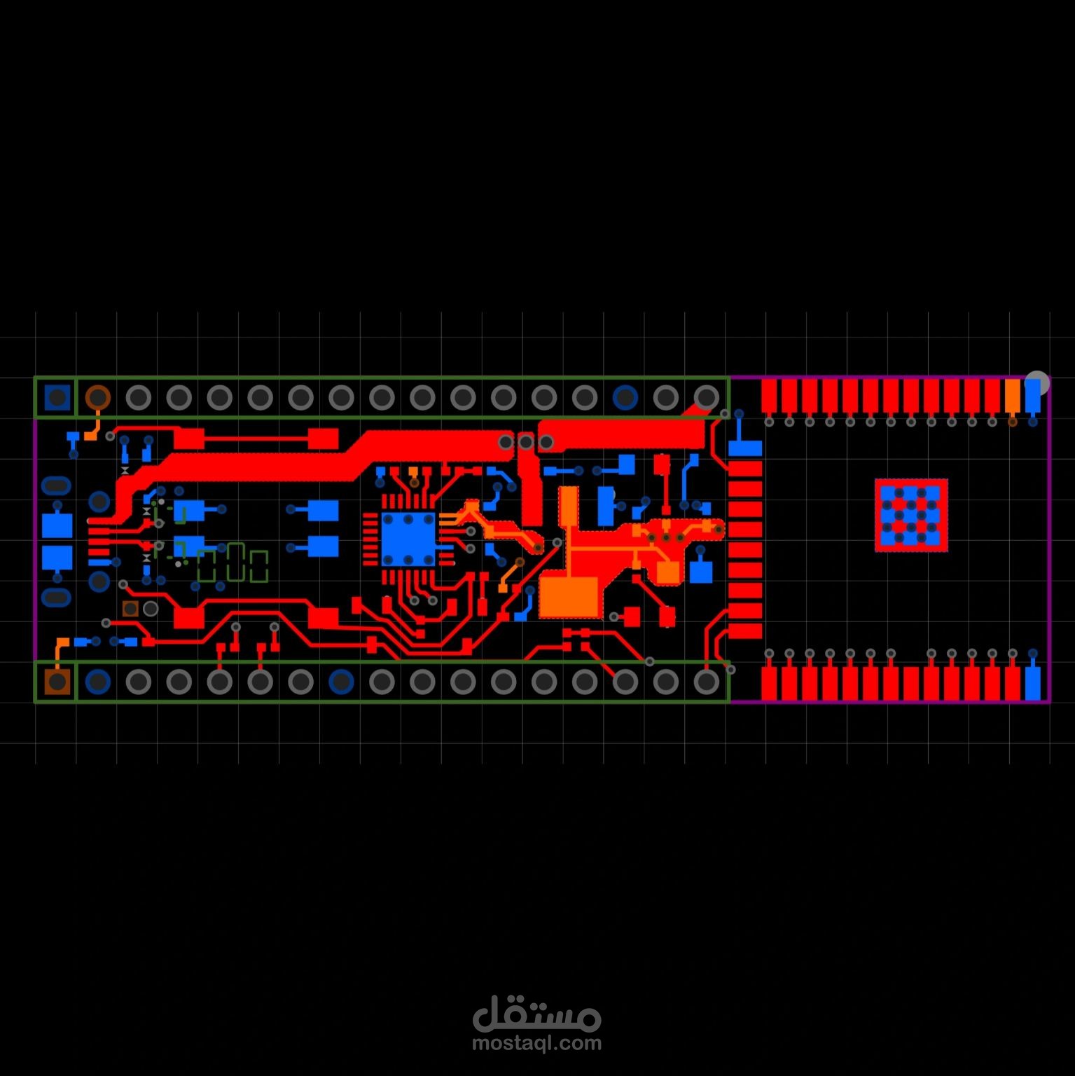
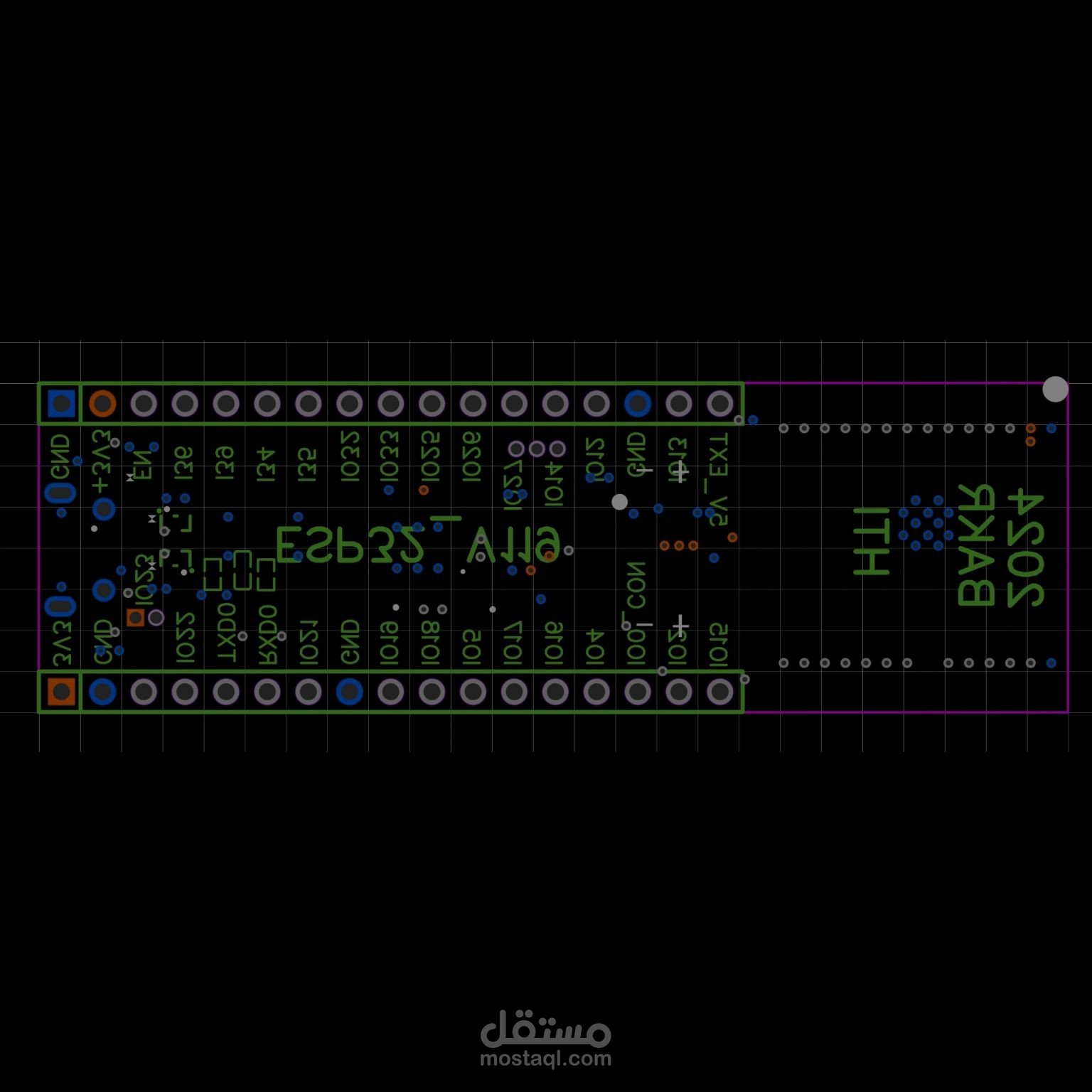
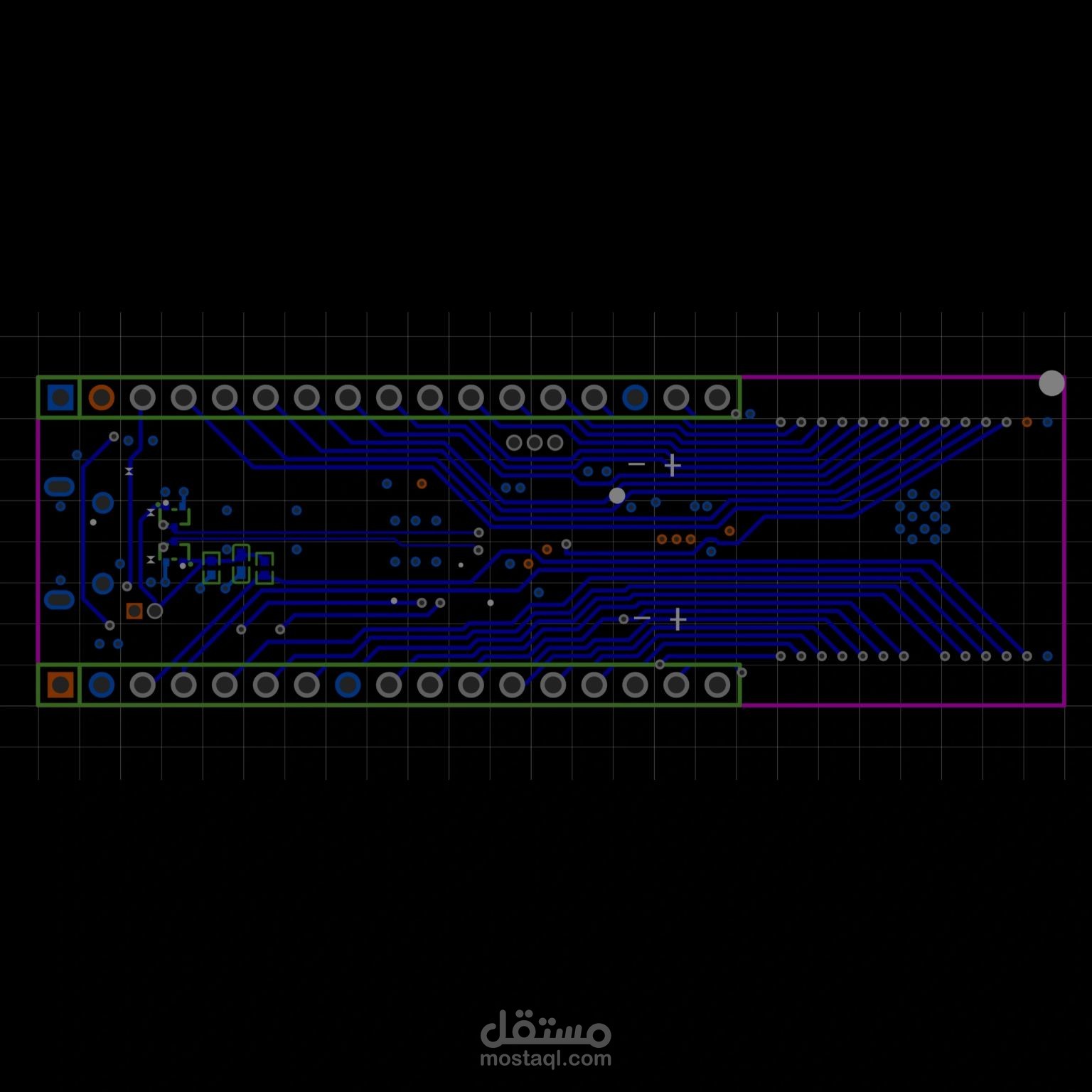
PCB Design & Selection Workflow
Understand Requirements – Define voltage, current, components, and board size.
Select Components – Choose microcontrollers, sensors, connectors, and power modules.
Schematic Design – Create the circuit diagram using ECAD tools (e.g., Altium, KiCad, Eagle).
PCB Layout – Place components, route traces, and optimize signal integrity.
Simulation & Verification – Check for design errors, EMI issues, and thermal management.
Prototype & Testing – Manufacture a sample PCB and validate performance.
Optimization & Finalization – Adjust design, improve efficiency, and prepare for production.
Production & Deployment – Mass manufacture, quality check, and implement in the system.